Purpose
The RT6266 is a high-efficiency, monolithic asynchronous step-down DC/DC converter with load line Compensation. This document explains the function and use of the RT6266 evaluation board (EVB) and provides information to enable operation and modification of the evaluation board and circuit to suit individual requirements.
Introduction
General Product Description
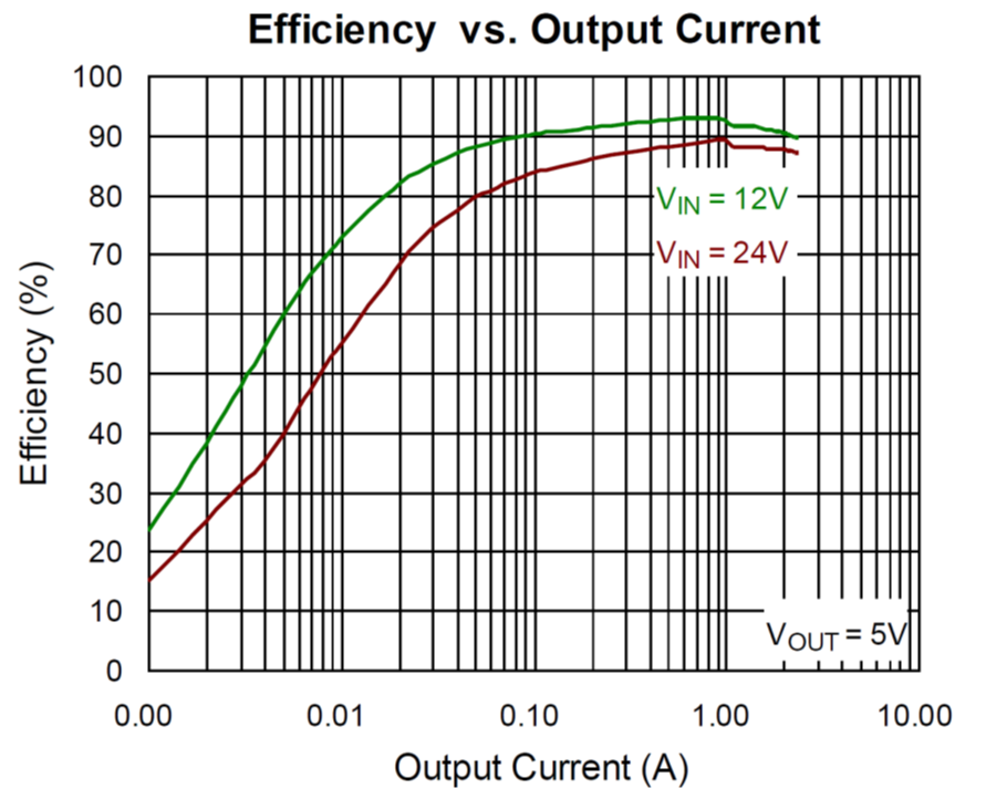
The RT6266 is a high-efficiency, monolithic asynchronous step-down DC/DC converter that can deliver up to 2.4A output current from a 7.5V to 36Vinput supply. The RT6266’s current mode architecture with internal compensation is optimized for 5V car charger application over a wide range of loads and output capacitors. Cycle-by-cycle current limit provides protection against shorted outputs and soft-start eliminates input current surge during start-up. The RT6266 also provides output over voltage protection output under voltage protection and thermal shutdown protection. The low current (<3μA) shutdown mode provides output disconnect, enabling easy power management in battery-powered systems. The RT6266 is available in a SOP-8 (Exposed Pad) package.
Product Features
- ±2% High Accuracy Feedback Voltage
- 7.5V to 36V Input Voltage Range
- 2.4A Continuous Output Current (2.7A Peak)
- CC/CV Mode Control
- Adjustable Load Line Compensation
- Short Circuit Protection
- Integrated N-MOSFET Switches
- Current Mode Control
- Fixed Frequency Operation : 100kHz
- Programmable Output Current Limit
- 110mΩ Internal Power MOSFET Switch
- Low EMI
- Up to 95% Efficiency
- Cycle-by-Cycle Over Current Protection
- Input Under Voltage Lockout
- Output Under Voltage Protection
- Thermal Shutdown Protection
Application
- USB Power Supplies
- Automotive Cigarette Lighter Adapters
- Power Supply for Linear Chargers
- DC/DC Converters with Current Limited
Evaluation Board
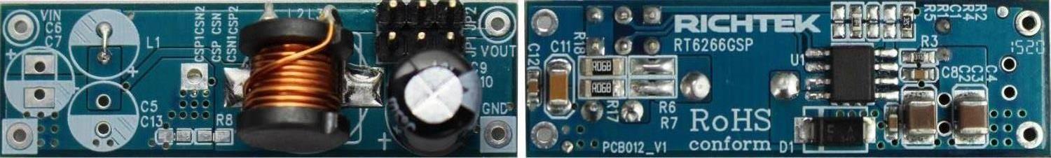
Please carefully inspect the EVB IC and external components, comparing them to the following Bill of Materials, to ensure that all components are installed and undamaged. If any components are missing or damaged during transportation, please contact the distributor or send e-mail to evb_service@richtek.com
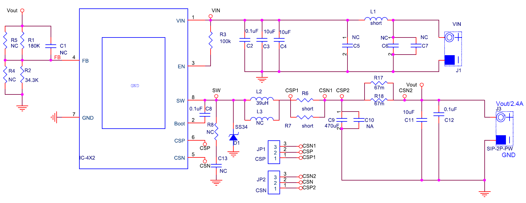
Test Points
The EVB is provided with the test points and pin names listed in the table below.
|
Test point/Pin name
|
Signal
|
Comment (expected waveforms or voltage levels on test points)
|
|
VIN
|
Input voltage
|
Input voltage range = 7.5V to 36V
|
|
VOUT
|
Output voltage
|
Output voltage = 5V
|
|
CSP
|
Current Sense Positive Input.
|
In this RT6266 EVB original setting, the CSP pin of JP1 should be connected short with CSN1 by jumper for normal operation.
|
|
CSN
|
Current Sense Negative Input.
|
In this RT6266 EVB original setting, the CSN pin of JP2 should be connected short with CSN2 by jumper for normal operation.
|
Power-up & Measurement Procedure
1. Connect input power (7.5V< VIN < 36V) and input ground to VIN pin.
2. Connect positive end and negative end of load to VOUT pin.
3. The output voltage of (Vout) can be set by R1 and R2.
Vout = VREF * (1+R1/R2)
where VREF = 0.8V (typ.)
Specification
|
Parameter
|
Symbol
|
Min
|
Typ.
|
Max
|
Units
|
|
Input Voltage Range
|
VIN
|
7.5
|
|
36
|
V
|
|
Output Voltage
|
VOUT
|
|
5
|
|
V
|
|
Oscillator Frequency
|
fOSC
|
85
|
100
|
115
|
kHz
|
|
Output Current
|
IOUT
|
|
|
2.4
|
A
|
|
Upper Switch Current Limit
|
ILIM
|
|
4.4
|
|
A
|
Schematic
BOM
|
Reference
|
Q'ty
|
P/N
|
Description
|
Package
|
Manufacture
|
|
U1
|
1
|
RT6266GSP
|
Step-down converter
|
SOP-8
|
RICHTEK
|
|
C2, C8, C12
|
3
|
C1608X7R1H104K080AA
|
0.1μF/±10%/50V/X7R
|
C-0603
|
TDK
|
|
C3, C4
|
2
|
C3216X5R1H106K160AB
|
10μF/±10%/50V/X5R
|
C-1206
|
TDK
|
|
C1, C5, C6, C7, C10, C13
|
6
|
|
NC
|
|
|
|
C9
|
1
|
GR, E-Cap
|
470μF/16V
|
|
CHI LI TEH
|
|
C11
|
1
|
C3216X7R1E106K
|
10uF/±10%/25V/X7R
|
C-1206
|
TDK
|
|
L1
|
1
|
|
Short
|
|
|
|
L2
|
1
|
MCD110C-390K-LV
|
39uH
|
|
MAG.LAYERS
|
|
L3
|
1
|
|
NC
|
|
|
|
D1
|
1
|
CDBA340-G
|
3A/40V
|
|
Comchip
|
|
R1
|
1
|
|
180k
|
|
|
|
R2
|
1
|
|
34.3k
|
|
|
|
R3
|
1
|
|
100k
|
|
|
|
R6, R7
|
2
|
|
Short
|
|
|
|
R17, R18
|
2
|
|
67m
|
|
|
|
R4, R5, R8
|
3
|
|
NC
|
|
|
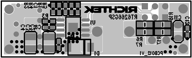
PCB Layout
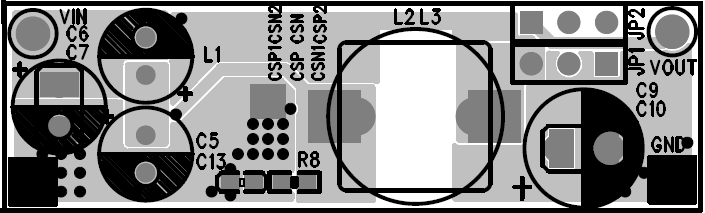
Top View
Bottom View
Step-Down Converter Efficiency Test